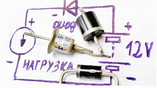
In this video, the PN junction diode has been explained. And the working of this PN junction diode under forward and reverse bias has been explained.
By watching this video, you will learn the following topics:
0:16 What is PN Junction Diode
1:48 The depletion region in the PN junction Diode
3:50 Unbiased PN Junction Diode
7:00 Forward-Biased PN Junction
9:46 Reverse Biased PN Junction
What is PN Junction Diode:
When the P-type and N-type semiconductors are grown on the same crystal then the junction is formed where this P-type and N-type region meets. And this junction is known as the PN Junction. And the entire structure acts as a diode.
The Depletion Region in PN Junction:
In PN junction diode, when p-type and n-type regions are joined together then electrons from the n-side recombines with the holes near the junction. And in this process, they create the positive and negative ions nears the junction. Hence, the region near the junction only contains positive and the negative ions. And being depleted from the free charge region, this region near the junction is knowns as the Depletion region.
The Unbiased PN Junction:
In the PN junction, the positive and the negative ions near the junction creates an electric field (Also knowns as the built-in electric field). This electric field prevents the majority carriers on both p-type and n-type region from diffusing through the depletion region.
So, the depletion region creates a barrier potential or built-in potential for majority carriers.
For, silicon this built-in potential is 0.7V and for germanium, it is 0.3V.
But due to this electric field, the minority carriers near the junction gets attracted towards the junction and swapped across the depletion region.
But under no biasing, the flow of minority charge carrier (due to the built-in electric field) and flow of majority carrier (due to diffusion) balances each other and net current in the circuit is zero.
The forward biased PN junction :
In forward biasing, the p-type terminal is connected to the positive terminal of the battery. While the n-type is connected to the negative terminal of the battery.
And as we increase the external biasing voltage, the width of the depletion region reduces. So, the resistance offered by the depletion region (to majority carrier reduces).
And once the applied voltage is more than the built-in potential, the majority carriers are able to cross this depletion region barrier.
So, under the forward bias condition, the current flows due to majority carriers. And the direction of the current is from p to n side. (Electrons moves from n-side to p-side and holes move from p-side to n-side)
The reversed biased PN Junction:
Under, reverse biased PN Junction, the p-side is connected to the negative terminal of the battery and n-side is connected to the positive terminal of the battery.
And as the reverse bias voltage increases, the width of the depletion region also increases. So, the resistance offered by the depletion region also increases.
But in the reverse bias condition, we get a flow of current due to minority carriers. Due to the strong electric field, the electrons get swapped from p-side to n-side and holes get swapped from n-side to p-side. So, in the reverse biased condition, we get a little flow of current due to minority carriers and the current flows from n-side to p-side. (In the reverse direction than the forward biased condition )
And that's why this current is known as the reverse saturation current.
This video will be helpful to all students of science and engineering in understanding the PN junction and how it works under forward and reverse biased condition.
#PNJunction
#ForwardBias
#ReverseBias
Follow me on YouTube:
[ Ссылка ]
Follow me on Facebook:
[ Ссылка ]
Follow me on Instagram:
[ Ссылка ]
Music Credit:
[ Ссылка ]
PN junction Diode Explained | Forward Bias and Reverse Bias
Теги
ALL ABOUT ELECTRONICSall about electronicsPN junction diode | Forward Bias and Reverse Biaspn junctionpn junction diodepn junction forward and reverse biasforward bias and reverse bias diodeforward bias and reverse biaspn junction diode workingpn junction diode theorypn junction diode theory forward and reverse biasworking of pn junction diodehow pn junction worksbiasing of pn junction diodediode forward and reverse biasall about electronics diode


