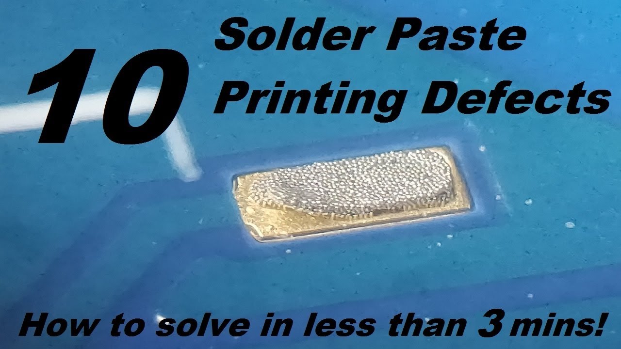
Solutions to 10 of the main solder paste printing process defects.
1) Excessive solder paste - Check PCB support - ideally use adaptable system, check stencil for damage, if label required to be fitted ensure located away from print area.
2) Poor print alignment - check alignment of PCB to stencil, check position/quality of fiducial marks on PCB and stencil, check machine settings.
3) Insufficient/partial print - Ensure solder paste fully conditioned, check aperture aspect ratio, consider using fine-grain material for stencil and/or nano-coating.
4) Scooping - Divide large stencil apertures into smaller. If using low-temperature, lead-free solder paste, ensure print speed fast enough.
5) Peaking - Check PCB separation speed not set too fast (should be set to a speed up to 3mm/sec), check stencil for damage.
6) Bridging - Check stenci for damage/cleanliness, correct stencil tension, good stencil design, ensure PCB has enough support, good temperature / humidity.
7) Paste in via's - If PCB mis-printed and needed to be re-printed, ensure fully cleaned with correct chemical under pressure.
8) Bleeding - Check gasketing seal between stencil and PCB (aperture should be smaller than pad), check PCB support, check stencil condition / cleanliness.
9) Slump - Check condition of paste and environment inside printer, consider the use of a temperature control module for the printer.
10) Incomplete paste fill for pin-in-hole - Ensure correct squeegee pressure and angle of 45 degrees, may need to double print.
[ Ссылка ]
#smt #soldering #defects


![Dziewczyny fortuny - RMF FM [WPADKA z 30.10.2009]](https://i.ytimg.com/vi/LVWQ8BnQabo/mqdefault.jpg)


